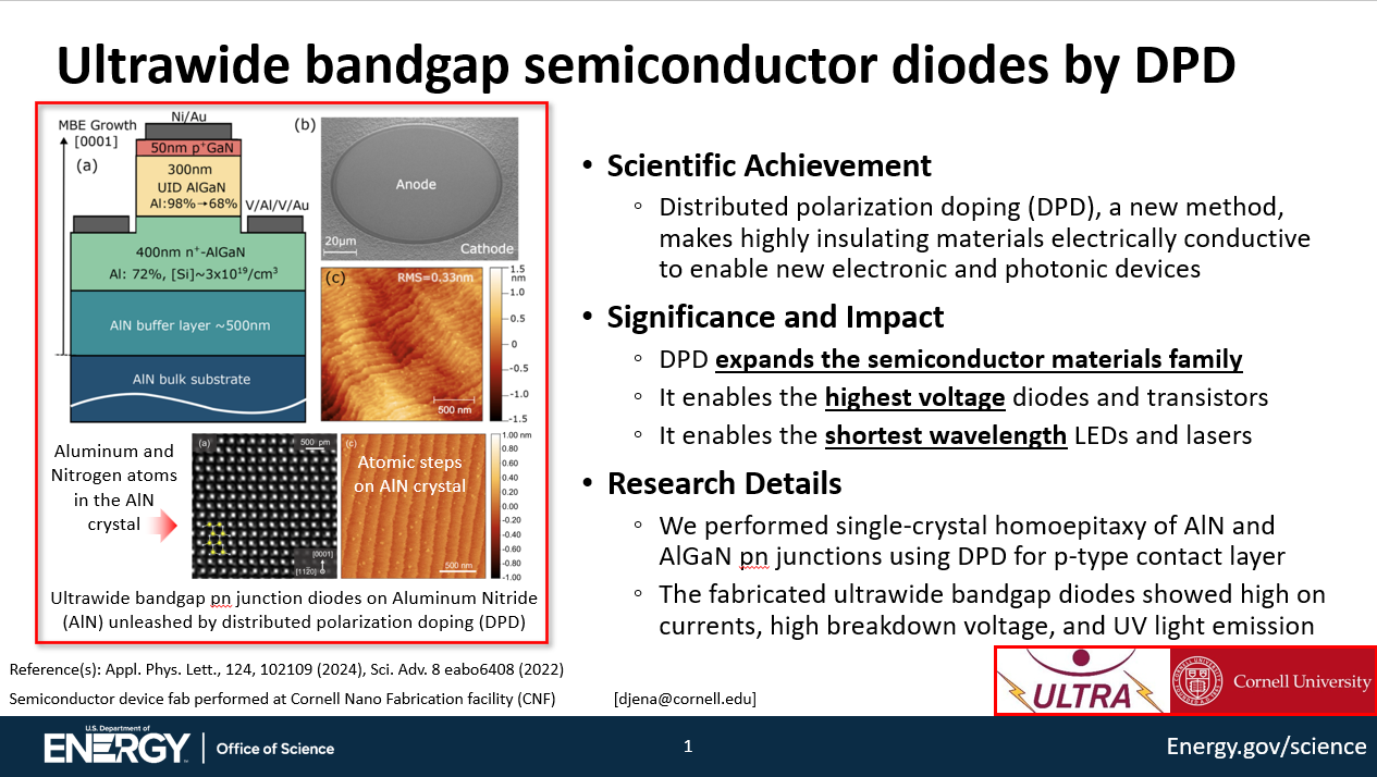
Ultrawide bandgap semiconductor diodes by DPD
Scientific Achievement
Distributed polarization doping (DPD), a new method, makes highly insulating materials electrically conductive to enable new electronic and photonic devices
Significance and Impact
DPD expands the semiconductor materials family
It enables the highest voltage diodes and transistors
It enables the shortest wavelength LEDs and lasers
Research Details
- We performed single-crystal homoepitaxy of AlN and AlGaN pn junctions using DPD for p-type contact layer
- The fabricated ultrawide bandgap diodes showed high on currents, high breakdown voltage, and UV light emission
Highlight provided by Debdeep Jena
Cornell University
February 2025
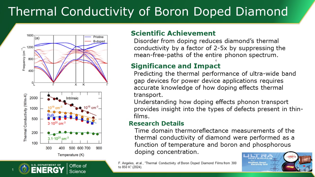
Thermal Conductivity of Boron Doped Diamond
Scientific Achievement
Disorder from doping reduces diamond’s thermal conductivity by a factor of 2-5x by suppressing the mean-free-paths of the entire phonon spectrum.
Significance and Impact
Predicting the thermal performance of ultra-wide band gap devices for power device applications requires accurate knowledge of how doping effects thermal transport.
Understanding how doping effects phonon transport provides insight into the types of defects present in thin-films.
Research Details
Time domain thermoreflectance measurements of the thermal conductivity of diamond were performed as a function of temperature and boron and phosphorous doping concentration.
Highlight provided by Richard Wilson
University of California, Riverside
May 2024
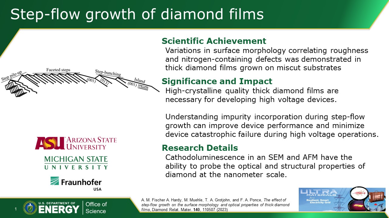
Step-flow growth of diamond films
Scientific Achievement
Variations in surface morphology correlating roughness and nitrogen-containing defects was demonstrated in thick diamond films grown on miscut substrates
Significance and Impact
High-crystalline quality thick diamond films are necessary for developing high voltage devices.
Understanding impurity incorporation during step-flow growth can improve device performance and minimize device catastrophic failure during high voltage operations.
Research Details
Cathodoluminescence in an SEM and AFM have the ability to probe the optical and structural properties of diamond at the nanometer scale.
Highlight provided by Alex Fischer
Arizona State University
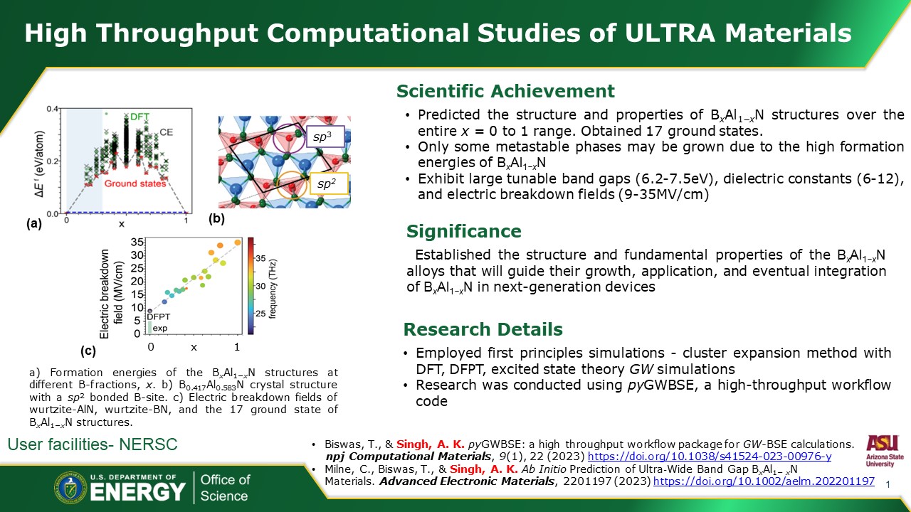
High Throughput Computational Studies of ULTRA Materials
Scientific Achievement
•Predicted the structure and properties of BxAl1−xN structures over the entire x = 0 to 1 range. Obtained 17 ground states.
•Only some metastable phases may be grown due to the high formation energies of BxAl1−xN
•Exhibit large tunable band gaps (6.2-7.5eV), dielectric constants (6-12), and electric breakdown fields (9-35MV/cm)
Significance and Impact
Established the structure and fundamental properties of the BxAl1−xN alloys that will guide their growth, application, and eventual integration of BxAl1−xN in next-generation devices.
Research Details
•Employed first principles simulations - cluster expansion method with DFT, DFPT, excited state theory GW simulations
•Research was conducted using pyGWBSE, a high-throughput workflow code.
Highlight given by Arunima Singh
Arizona State University
July 2023

Diamond Photoconductive Switches for High Voltage
Scientific Achievement
Extrinsic photoconductive switching was demonstrated in nitrogen and boron doped diamond in response to below bandgap light.
Significance and Impact
Diamond is an ultra wide bandgap semiconductor with properties that can enable more compact and efficient devices.
Diamond-based photoconductive switches (PCSS) can contribute to more resilient grid-level electronics due to its high voltage capabilities and isolated triggering.
Research Details
Using 532 and 1064 nm laser pulses, the photoconductivity of diamond was analyzed and attributed to the excitation of carriers in deep dopant states to the conduction and valence bands.
Highlight given by Kelly Woo
Stanford University
June 2023
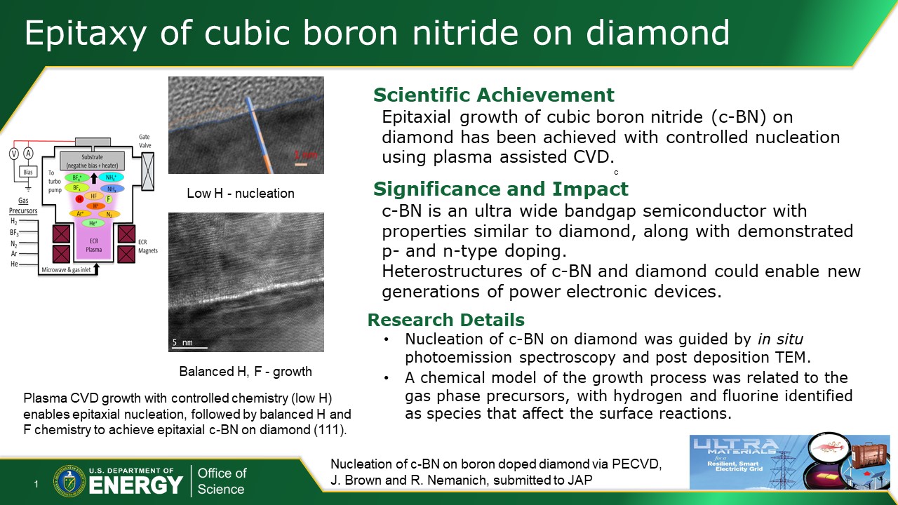
Epitaxy of Cubic Boron Nitride on Diamond
Scientific Achievement
Epitaxial growth of cubic boron nitride (c-BN) on diamond has been achieved with controlled nucleation using plasma assisted CVD.
Significance and Impact
c-BN is an ultra wide bandgap semiconductor with properties similar to diamond, along with demonstrated p- and n-type doping.
Heterostructures of c-BN and diamond could enable new generations of power electronic devices.
Research Details
- Nucleation of c-BN on diamond was guided by in situ photoemission spectroscopy and post deposition TEM
- A chemical model of the growth process was related to the gas phase precursors, with hydrogen and fluorine identified as species that affect the surface reactions
Highlight given by Robert Nemanich
Arizona State University
May 2022
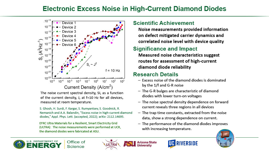
Electronic Excess Noise in High-Current Diamond Diodes
Scientific Achievement
Noise measurements provided information on defect mitigated carrier dynamics and correlated noise level with device quality
Significance and Impact
Measured noise characteristics suggest routes for assessment of high-current diamond diode reliability
Research Details
- Excess Noise of the diamond diodes is dominated by the 1/f and G-R noise
- The G-R bulges are characteristic of diamond diodes with lower turn-on voltages in all devices
- The trap time constants, extracted from the noise data, show a strong dependence on current
- The performance of the diamond diodes improves with increasing temperature
Highlight given by Alexander Balandin
University of California, Riverside
February 2022
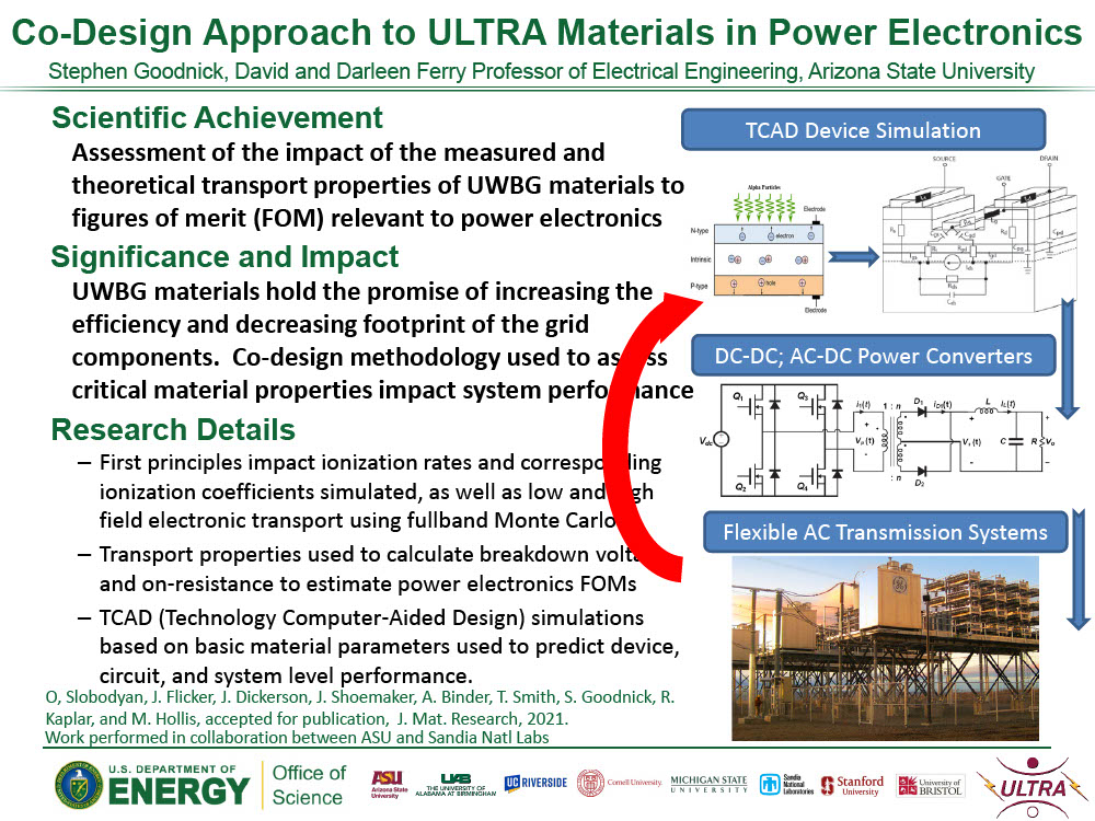
Co-Design Approach to ULTRA Materials in Power Electronics
Scientific Achievement
Assessment of the impact of the measured and theoretical transport properties of UWBG materials to figures of merit (FOM) relevant to power electronics
Significance and Impact
UWBG materials hold the promise of increasing the efficiency and decreasing footprint of the grid components. Co-design methodology used to assess critical material properties impact system performance
Research Details
- First principles impact ionization rates and corresponding ionization coefficients simulated, as well as low and high field electronic transport using fullband Monte Carlo
- Transport properties used to calculate breakdown voltage and on-resistance to estimate power electronics FOMs
- TCAS (Technology Computer-Aided Design) simulations based on basic material parameters used to predict device, circuit, and system level performance
Highlight given by Stephen Goodnick
Arizona State University
November 2021
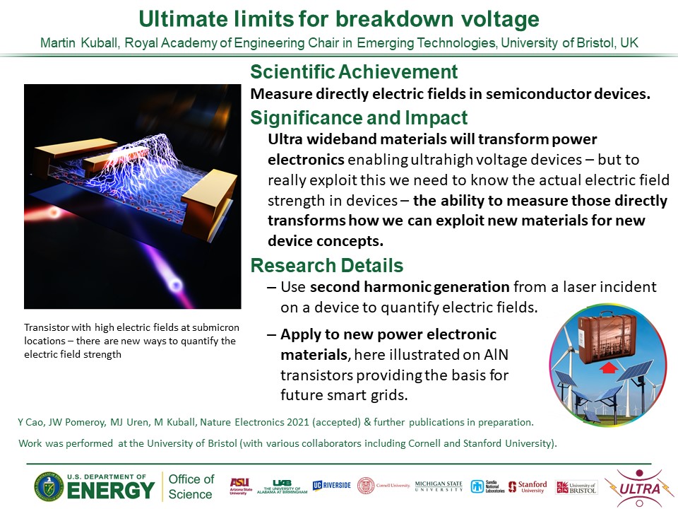
Ultimate Limits for Breakdown Voltage
Scientific Achievement
Measure directly electric fields in semiconductor devices
Significance and Impact
Ultra wideband materials will transform power electronics enabling ultrahigh voltage devices - but to really exploit this we need to know the actual electric field strength in devices - the ability to measure those directly transforms how we can exploit new materials for new device concepts
Research Details
- Use second harmonic generation from a laser incident on a device to quantify electric fields
- Apply to new power electronic materials, here illustrated on A|N transistors providing the basis for future smart grids
- Highlight Provided by Martin Kuball
- University of Bristol
- June 2021
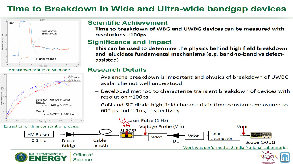
Time to Breakdown in Wide and Ultra-wide Bandgap Devices
Scientific Achievement
Time to breakdown of WBG and UWBG devices can be measured with resolutions ~100ps
Significance and Impact
This can be used to determine the physics behind high field breakdown and elucidate fundamental mechanisms (e.g. band-to-band vs defect-assisted)
Research Details
- Avalanche breakdown is important and physics of breakdown of UWBG avalanche now well understood
- Developed method to characterize transient breakdown of devices with resolution ~100ps
- GaN and SiC diode high field characteristic time constats measured to 600ps and ~1ns, respectively
Highlight given by Jack Flicker
Sandia National Laboratories
April 2021
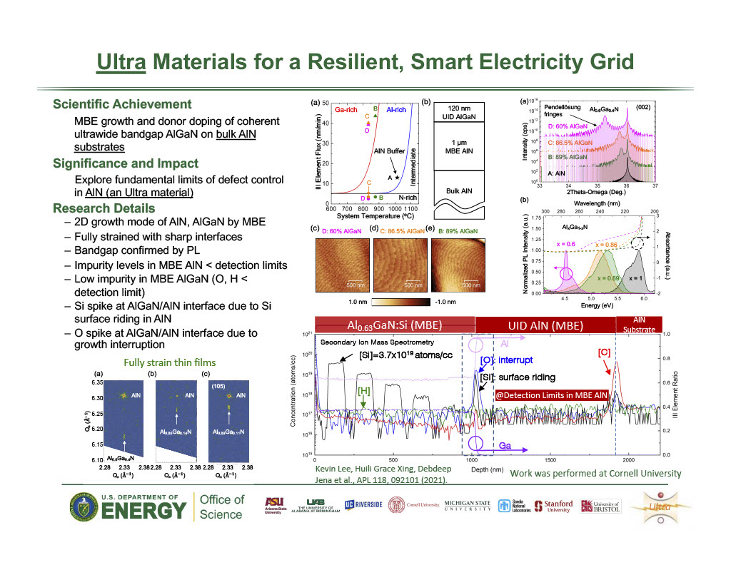
MBE Growth and Donor Doping of Coherent Ultrawide Bandgap AlGaN on Bulk AlN Substrates
Scientific Achievement
MBE growth and donor doping of coherent ultrawide bandgap AlGaN on bulk AlN substrates
Significance and Impact
Explore fundamental limits of defect control in AlN (an Ultra material)
Research Details
- 2D Growth mode of AIN, AIGaN, by MBE
- Fully strained with sharp interfaces
- Bandgap confirmed by PL
- Impurity levels in MBE AIN < detection limits
- Low impurity in MBE AIGaN (O, H < detection limit)
- Si spike at AIGaN/AIN interface due to Si surface riding in AIN
Highlight provided by Grace Xing
Cornell University
January 2021